|
The 18th
International Workshop on Junction Technology (IWJT2018) will be held
on March 8 - 9, 2018 in Shanghai, China.
The date for IWJT-2018 is scheduled to connect with the China
Semiconductor Technology International Conference (CSTIC)
2018 which will be held on March 11-12, 2018 in Shanghai too.
The IWJT, started in 2000 and
was held annually in Japan or China, is an open forum focused on the needs
and interest of the community of a junction formation technology in
semiconductors. At the past IWJTs, a number of eminent and experienced
scientists and engineers from Asia, America, and Europe presented their
latest results on junction technology. The workshop will provide a good
opportunity for researchers and engineers to present their new research
results, and exchange ideas with leading scientists in this
field.
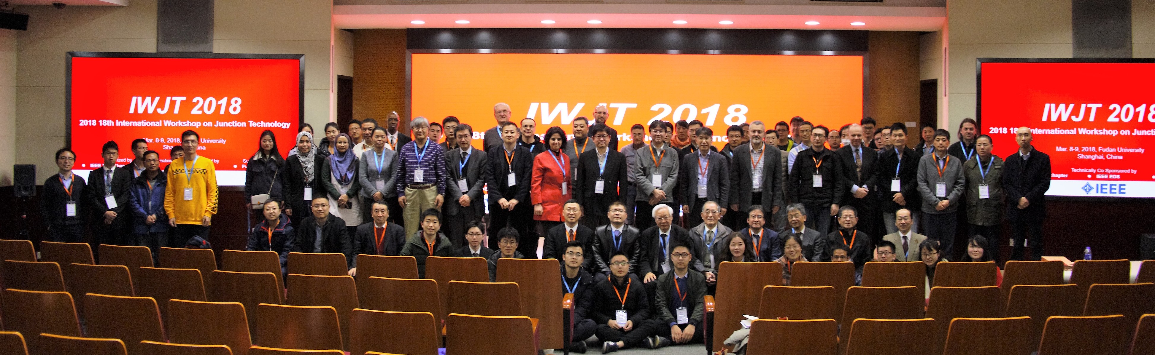
(Group Photo, IWJT2018, Mar.
8, 2018)
On site registration:
Room 102, 1st floor, East Auxiliary Building Affiliated
to Guanghua Building
15:00-18:00, Mar. 7, 2018
08:00-11:30, Mar. 8, 2018
08:00-11:30, Mar. 9, 2018
Only cash is acceptable. No payment by
bank card is available.
 Overview
Schedule Overview
Schedule
| |
Mar. 8, Thursday |
Mar. 9, Friday |
|
Morning |
Opening & Plenary Session
(08:30-10:30)
Characterization
for Shallow Junction
(10:45-12:00)
Registration
(8:00-11:30) |
Doping Technology
(8:30-10:00)
Metal/Semiconductor
Contact Technology for CMOS
(10:15-11:45)
Registration
(8:00-11:30) |
|
Lunch |
Danyuan restaurant, 3rd floor
(12:00-13:15) |
Danyuan restaurant, 3rd floor
(12:00-13:15) |
|
Afternoon |
Annealing Technology
(13:30-15:15)
Junction and Contact Technologies for Compound
Semiconductors
(15:30-17:30) |
Contact and Junction Technologies for photon-electron
interaction
(13:30-15:45)
Modeling
and Simulation
(16:00-16:45)
Junction
and Process Technology for Novel MOS Device Structures
(16:45-18:00) |
|
Evening |
Danyuan restaurant, 3rd floor
Reception
(18:00-19:30) |
Danyuan restaurant, 3rd floor
Banquet
(18:00-19:30) |
Final
Program
(20180228)
|
Mar. 8 (Thur.)
08:30-09:00 |
Opening
(Room 102, 1st floor, East Auxiliary Building Affiliated
to Guanghua Building) |
|
|
Mar.
8 (Thur.)
09:00-10:30 |
Plenary Session
(Room 102, 1st floor, East Auxiliary Building Affiliated
to Guanghua Building) |
|
|
Co-Chairs: |
Bing-Zong Li, Fudan University, China
Mizuno Bunzi, Panasonic, Japan |
|
|
K1 |
Advanced Implant Application for 7nm and Beyond |
1 |
|
9:00 |
Wei (David) Zou, Kyu-Ha Shim and Todd Henry |
|
|
(Keynote) |
AMAT, USA |
|
|
K2 |
Impact of the end of CMOS miniaturization on ICT and the world after
that |
2 |
|
9:45 |
Hiroshi Iwai |
|
|
(Keynote) |
Tokyo Institute of Technology, Japan |
|
|
Coffee Break (10:30-10:45) |
|
Mar.
8 (Thur.)
10:45-12:00 |
Characterization for Shallow Junction
(Room 102, 1st floor, East Auxiliary Building Affiliated
to Guanghua Building) |
|
|
Chair: |
Kyoichi Suguro, Toshiba, Japan |
|
|
S01-01 |
Analyses of 3D Atomic Arrangements of Impurity Atoms Doped in
Silicon by Spectro-Photoelectron Holography Technique |
7 |
|
10:45 |
Kazuo Tsutsui1, Tomohiro Matsushita2, Takayuki
Muro2, Yoshitada Morikawa3, Kotaro Natori4,
Takuya Hoshii4, Kuniyuki Kakushima4, Hitoshi
Wakabayashi4, Kouichi Hayashi5, Fumihiko
Matsui6, and Toyohiko Kinoshita2 |
|
|
(Invited) |
1Institute
of Innovative Research, Tokyo Institute of Technology, Japan; 2
Japan Synchrotron Radiation Research Institute (JASRI), Japan;
3 Osaka University, Japan; 4School of Engineering,
Tokyo Institute of Technology, Japan; 5Nagoya Institute
of Technology, Japan; 6 Nara Institute of Science and
Technology, Japan |
|
|
S01-02 |
Junction profiling on hot carrier stressed device by dual lens
electron holography and scanning capacitance microscopy |
13 |
|
11:15 |
Y.Y. Wang 1, J. Nxumalo1, D. Ioannou1,
A. Katnani1, J. Jeon1, K. Bandy1, M. Mcdonald1,
J. Bruley2 |
|
| |
1.
Globalfoundires Inc., USA; 2. IBM T. J. Watson Research
Center, USA |
|
|
S01-03 |
Characterizing Junction Profiles in Ge Photodetectors using Scanning
Capacitance Microscopy (SCM) and Electron Holography |
17 |
|
11:30 |
J. N. Nxumalo1, Y.Y. Wang2, M. Iwatake2,
C. Molella1, A. Katnani2, J. Orcutt3,
J. Ayala2, K. Nummy2 |
|
| |
1GlobalFoundries
Inc., USA;2GlobalFoundries Inc., USA;3 IBM
Thomas J. Watson Research Center, USA |
|
|
S01-04 |
Effect of Stress on Activation during the Formation of np Junction
in Co-Implanted Germanium |
21 |
|
11:45 |
Nur Nadhirah Rashid1, Umar Abdul Aziz1, Siti
Rahmah Aid1, Suwa Akira2, Hiroshi Ikenoue2,
Fang Xie3 and Anthony Centeno4 |
|
| |
1Universiti
Teknologi, Malaysia;2Kyushu University, Japan;3Imperial
College London, United Kingdom;4Xi’an Jiaotong Liverpool
University, China |
|
|
Mar.
8 (Thur.)
13:30-15:15 |
Annealing Technology
(Room 102, 1st floor, East Auxiliary Building Affiliated
to Guanghua Building) |
|
|
Co-Chairs: |
Paul J. Timans,
Mattson Thermal Products GmbH, Germany
S. Boninelli,
IMM-CNR, Italy |
|
|
S02-01 |
Activation of High-temperature-implanted Phosphorus Atoms in 4H-SiC
by Atmospheric Pressure Thermal Plasma Jet Annealing |
24 |
|
13:30 |
H. Hanafusa and S. Higashi |
|
|
(Invited) |
Hiroshima University, Japan |
|
|
S02-02 |
Activation Trends in Millisecond Annealing of Heavy n-Type Doping of
Silicon |
28 |
|
14:00 |
Paul J. Timans |
|
|
(Invited) |
Mattson Thermal Products GmbH, Germany |
|
|
S02-03 |
Damage recovery and strain induced by Phosphorous in Laser Annealed
Ge |
32 |
|
14:30 |
S. Boninelli1, and F. Cristiano2 |
|
|
(Invited) |
1IMM-CNR,
Italy; 2LAAS-CNRS, France |
|
|
S02-04 |
High Activation Reaching Supersaturation Achieved by Short-Duration
Flash Lamp Annealing |
33 |
|
15:00 |
Hideaki Tanimura, Kenji Inoue, Hikaru Kawarazaki, Takahiro Yamada,
Kazuhiko Fuse, Takayuki Aoyama, Shinichi Kato and Ippei Kobayashi |
|
| |
SCREEN Semiconductor Solutions Co., Ltd., Japan |
|
|
Coffee Break (15:15-15:30) |
|
Mar.
8 (Thur.)
15:30-17:30 |
Junction and Contact Technologies for Compound Semiconductors
(Room 102, 1st floor, East Auxiliary Building Affiliated
to Guanghua Building) |
|
|
Co-Chairs: |
Hongyu Yu,
Southern University of Science and Technology, China
Philippe Rodriguez,
Univ. Grenoble Alpes, France |
|
|
S03-01 |
Au-based and Au-free Ohmic Contacts to AlGaN/GaN Structures on
Silicon or Sapphire Substrates |
37 |
|
15:30 |
Wenmao Li1,2, Jian Zhang3, Robert Sokolovskij1,2,4,5,
Yumeng Zhu1,2, Yongle Qi1,2, Xinpeng Lin1,2,
Jingyi Wu1,2, Lingli Jiang1,2, Hongyu Yu1,2 |
|
|
(Invited) |
1
Southern University of Science and Technology, China; 2Shenzhen
Key Laboratory of the Third Generation Semi-conductor, China; 3Fudan
University, China; 4Delft University of Technology, the
Netherlands; 5State Key Laboratory of Solid State
Lighting, China |
|
|
S03-02 |
CMOS-Compatible Contact Technology for Si Photonics |
41 |
|
16:00 |
Philippe Rodriguez1, Elodie Ghegin2, and
Fabrice Nemouchi3 |
|
|
(Invited) |
1Univ.
Grenoble Alpes, France; 2 CEA-LETI, France; 3
STMicroelectronics, France |
|
|
S03-03 |
Characterization of b-Ga2O3 Schottky Barrier
Diodes |
47 |
|
16:30 |
T. Kaneko1, I. Muneta1, T. Hoshii1,
H. Wakabayashi1, K. Tsutsui2, H. Iwai2,
K. Kakushima1 |
|
| |
1School
of Engineering, Tokyo Institute of Technology, Japan; 2Institute
of Innovative Research, Tokyo Institute of Technology, Japan |
|
|
S03-04 |
Effect of Deep Level Traps on the I-V and C-V Characteristics of
InP/InGaAs Heterojunction |
50 |
|
16:45 |
Man-Li Zhao, Hong-Liang Lu, Yu-Ming Zhang, Yi-Men Zhang, Xiao-Hong
Zhao |
|
| |
Xidian University, China |
|
|
S03-05 |
The effect of ZnO Interface Passivation Layer on Leakage Current
Mechanisms and Band Alignment for ZrO2/In0.2Ga0.8As Metal Oxide
Semiconductor Capacitor |
54 |
|
17:00 |
TongYang, Hong-liang Lu, Chen Liu, Wei-jian Yu, Yu-ming Zhang,
Yi-men Zhang |
|
| |
Xidian University, China |
|
|
S03-06 |
Optimized transport properties of GaN MISHEMTs with thin AlN
interlayer |
59 |
|
17:15 |
Qianlan Hu, Sichao Li, Tiaoyang Li, Xin Wang, and Yanqing Wu |
|
| |
Huazhong University of Science and Technology, China |
|
|
Mar.
9 (Fri.)
08:30-10:00 |
Doping Technology
(Room 102, 1st floor, East Auxiliary Building Affiliated
to Guanghua Building) |
|
|
Chair: |
Hiro
Ito, AMAT, Japan |
|
|
S04-01 |
H2 PLAD Hydrogenation Process on 3D NAND Array Poly-Si
Access Devices |
61 |
|
8:30 |
Shu Qin |
|
|
(Invited) |
QinTek, Co., USA |
|
|
S04-02 |
Monolayer doping and other strategies in high surface-to-volume
ratio silicon devices |
65 |
|
9:00 |
Ray Duffy1, Noel Kennedy2, Gioele Mirabelli1,
Emmanuele Galluccio1, Paul K. Hurley1,2,
Justin D. Holmes2,3, and Brenda Long2 |
|
|
(Invited) |
1
Tyndall National Institute, Ireland; 2 University College
Cork, Ireland. 3 Trinity College Dublin, Ireland. |
|
|
S04-03 |
Enhancing Phosphorous Doping Level on Ge by Sb co-Doping with
Non-Beamline Implantation Methods |
71 |
|
9:30 |
Chuck Paeng, He Zhang, Bodo Kalkofen*, and YS Kim |
|
| |
Lam Research Corp., USA; *U. Magdeburg Otto-von-Guericke |
|
|
S04-04 |
Atomic layer deposited solid sources for doping of high aspect ratio
semiconductor structures |
75 |
|
9:45 |
Bodo Kalkofen1, Mindaugas Šilinskas1, Marco
Lisker2, Y. S. Kim3, and Edmund P. Burte1 |
|
| |
1
Otto von Guericke University, Germany;2 IHP, Germany;3
Lam Research Corporation, USA |
|
|
Coffee Break (10:00-10:15) |
|
Mar.
9 (Fri.)
10:15-11:45 |
Metal/Semiconductor Contact Technology for CMOS
(Room 102, 1st floor, East Auxiliary Building Affiliated
to Guanghua Building) |
|
|
Co-Chairs: |
Kuniyuki Kakushima, Tokyo Institute of Technology, Japan
Hao Yu,
IMEC, Belgium |
|
|
S05-01 |
On the manifestation of Ge Pre-amorphization Implantation (PAI)
Impact on Both the Formation of Ultrathin TiSix and the Specific
Contact Resistivity in TiSix/n-Si Contacts for sub-16/14 nm nodes
and beyond |
79 |
|
10:15 |
Jun Luoa,b, Shujuan Maoa,b, Jing Xua,
Guilei Wanga, Dan Zhanga,b, Xue Luoa,b,
Ningyuan Duana,b, Shi Liua, Wenwu Wanga,b,
Dapeng Chena, Junfeng Lia, Chao Zhaoa,b,
Tianchun Yea,b |
|
|
(Invited) |
a
Institute of Microelectronics, Chinese Academy of Sciences, China;
bUniversity of Chinese Academy of Sciences (UCAS), China |
|
|
S05-02 |
Titanium (Germano-)Silicides Featuring 10-9
Ω∙cm2
Contact Resistivity and Improved Compatibility to Advanced CMOS
Technology |
80 |
|
10:45 |
Hao Yu1,2, Marc Schaekers1, Soon Aik Chew1,
Jean-Luc Everaert1, Naoto Horiguchi1, Dan
Mocuta1, Nadine Collaert1, Kristin De Meyer1,2 |
|
|
(Invited) |
1Imec,
Belgium; 2K. U. Leuven, Belgium |
|
|
S05-03 |
Improved thermal stability of Al/TiO2/n-Ge ohmic contact by
inserting single layer graphene |
85 |
|
11:15 |
Yi Zhang, Genquan Han, Jiabo Chen, Yan Liu, Jincheng Zhang, and Yue
Hao |
|
| |
Xidian University, China. |
|
|
S05-04 |
Effect of platinum interlayer on the thermal stability improvement
of nickel stanogermanide |
88 |
|
11:30 |
Weijun Wan1,2, Wei Ren1, Xiaoran Meng2,3,
Yunxia Ping3, Xing Wei2, Zhongying Xue2,
Wenjie Yu2, Miao Zhang2, Zengfeng Di2,
Bo Zhang2 |
|
| |
1Shanghai
University, China;2Shanghai Institute of Microsystem and
Information Technology, Chinese Academy of Sciences, China;3Shanghai
University of Engineering Science, China |
|
|
Mar.
9 (Fri.)
13:30-15:45 |
Contact and Junction Technologies for photon-electron interaction
(Room 102, 1st floor, East Auxiliary Building Affiliated
to Guanghua Building) |
|
|
Co-Chairs: |
Kenji Araki,
Toyota Technological Institute, Japan
Hitoshi Wakabayashi, Tokyo Institute of Technology,
Japan |
|
|
S06-01 |
Novel photodetector based on FD-SOI substrate with interface
coupling effect |
91 |
|
13:30 |
J. Wan1, JN. Deng1, XY. Cao1, H. B.
Liu1, B. R. Lu1, Y. F. Chen1, A.
Zaslavsky2, S. Cristoloveanu3 and M. Bawedin3 |
|
|
(Invited) |
1Fudan
University, China; 2Brown University, USA; 3IMEP-LAHC,
France |
|
|
S06-02 |
Opportunities for breaking an energy generation limit of
photovoltaic using multijunction and super-multijunction cells |
95 |
|
14:00 |
Kenji Araki, Kan-Hua Lee, and Masafumi Yamaguchi, |
|
|
(Invited) |
Toyota Technological Institute, Japan |
|
|
S06-03 |
Light Plastic Integrated Micro CPV Module: PIC with Three-Junction
PV cells |
99 |
|
14:30 |
Michihiko Takase, Masaharu Terauchi, Nobuhiko Hayashi, Hikaru
Nishitani, Takuji Inohara, Youichirou Aya, Shutetsu Kanayama and
Bunji Mizuno |
|
|
(Invited) |
Panasonic Corporation, Japan |
|
|
S06-04 |
Interfacial passivation by LiF or PbF2 for high efficiency
perovskite solar cell |
102 |
|
15:00 |
Yiqiang Zhan |
|
|
(Invited) |
Fudan University, China |
|
|
S06-05 |
Photodetector Based on Silicon-on-Insulator with High Responsivity |
103 |
|
15:30 |
X. Y. Cao1,2, HB.Liu1, JN.Deng1,
WS.Lin2,and J. Wan1 |
|
| |
1Fudan
University, China;2 Shanghai University of Engineering
Science, China |
|
|
Coffee Break (15:45-16:00) |
|
Mar.
9 (Fri.)
16:00-16:45 |
Modeling and Simulation
(Room 102, 1st floor, East Auxiliary Building Affiliated
to Guanghua Building) |
|
|
Chair: |
Dong-Ping Wu,
Fudan University, China |
|
|
S07-01 |
Parasitic Resistance Modeling and Optimization for 10nm-node FinFET |
107 |
|
16:00 |
Xicheng Duan, Peng Lu, Weicong Li, Jason C.S. Woo |
|
| |
University of California, USA |
|
|
S07-02 |
Simulation of Ge/(Si)GeSn Hetero-junction Tunnel FETs with
Suppressed Ambipolar Current6 |
111 |
|
16:15 |
Yongwang Zhang, Suyuan Wang, Jun Zheng, Chunlai Xue, Chuanbo Li,
Yuhua Zuo, Buwen Cheng, Qiming Wang |
|
| |
Institute of Semiconductors, Chinese Academy of Sciences and
University of Chinese Academy of Sciences |
|
|
S07-03 |
Thermal Failure and Voltage Overshoot Models for Diode Behavior
under Electrostatic Discharge Stresses |
115 |
|
16:30 |
Hang Li1, Yuanzhong Zhou2, Meng Miao1,
Javier A. Salcedo2, Jean-Jacques Hajjar2, and
Kalpathy B. Sundaram1 |
|
| |
1University
of Central Florida, USA;2Analog Devices, Inc., USA |
|
|
Mar.
9 (Fri.)
16:45-18:00 |
Junction and Process Technology for Novel MOS Device Structures
(Room 102, 1st floor, East Auxiliary Building Affiliated
to Guanghua Building) |
|
|
Chair: |
Jing Wan,
Fudan University, China |
|
|
S08-01 |
Gate stack and Ni(SiGeSn) metal contacts formation on low bandgap
strained (Si)Ge(Sn) semiconductors |
119 |
|
16:45 |
D. Buca1, C. Schulte-Braucks1, N. von den
Driesch1, A. T. Tiedemann1, U. Breuer2,
J.M. Hartmann3, P. Zaumseil4, S. Mantl1
and Q.T. Zhao1 |
|
|
(Invited) |
1Peter
Grünberg Institute (PGI 9) and JARA-FIT, Forschungszentrum, Germany;
2Central Division of Analytical Chemistry (ZCH),
Forschungszentrum, Germany;3 CEA-LETI, France; 4
IHP, Germany |
|
|
S08-02 |
High-performance heterojunctions based on 2D semiconductors |
120 |
|
17:15 |
Mingqiang Huang, Xiong Xiong and Yanqing Wu |
|
|
(Invited) |
Huazhong University of Science and Technology, China |
|
|
S08-03 |
Highly Selective Etch of Silicon Dioxide with Tungsten Hard Mask
Deposited by PVD Process |
122 |
|
17:45 |
Yuanhui Fang, Jian Zhang, and Yu-Long Jiang |
|
| |
Fudan University, China |
|
Call
for Papers
(PDF)
Important
Dates Deadline for Camera-Ready Full-Length Paper Submission :
Jan. 31, 2018
Notification of Regular Paper Acceptance: Feb. 15, 2018
Deadline for
Late News Submission
Extended:
Jan. 31, 2018
submission at web-site
Email submission with a cover letter to
iwjt@fudan.edu.cn is preferred.
Workshop Scope
(Papers are solicited in,
but not limited to the following)
-
Doping Technology --- Ion
implantation, plasma doping, gas and solid doping
-
Annealing Technology --- Rapid
thermal process, laser annealing, flash annealing, SPE, lattice damage
and defects
-
Junction Technology for Novel CMOS Device
Structures --- Junction for SOI, strained
Si, SiGe, Ge, Schottky barrier S/D MOSFET,
FinFET(Tri-gate FET), and bonding junctions -
Silicide and Contact Technology for
CMOS --- Silicide materials and salicide technology, elevated S/D,
low barrier contact, surface pre-treatment -
Junction and Contact Technologies for Compound Semiconductors and
Quantum Devices --- Schottky and ohmic contacts to wide bandgap
compound semiconductors, junction and contact technologies for carbon
nanotube, graphene, 2D material and other
2D or nano-, quantum
devices, hetero-junction devices -
Contact
and Junction Technologies for Energy Harvesting Devices---solar
cells -
Characterization for Shallow Junction
--- Physical and electrical characterization of ultra-shallow junction
-
Modeling and Simulation --- Modeling
and simulation of ultra-shallow junction formation of CMOS
-
Equipment, Materials and Substrates for
Junction Technology
Organized by
IEEE EDS Shanghai Chapter
IEEE EDS Japan Chapter
Technical Co-Sponsored by
IEEE EDS
Supported by
Fudan University

|